本次美国代写是模拟集成电相关的的一个assignment
In this assignment you will be designing and simulating a two stage amplifier as shown in Fig. 1. You also have to choose the sizes of the transistors. As a starting point, you could choose the width and length of all the transistors to be 60 µm and 30 µm respectively. Assume Vdd = 3V and the maximum load connected to the output is 1pF.
1. Use DC analysis to determine the gain of the amplifier. Remember for DC analysis, set Vin- to 1.5V and then sweep Vin+ from 0 to 3V. Repeat this for bias current Ib values of 1nA ,10nA, 100nA, 1μA. The value of the capacitor C should not affect the DC analysis [10 point].
2. Using the amplifier create a voltage follower (buffer) as shown in Fig. 1 (right). Apply a 100μV step input (1.4995V – 1.5005V) (see Fig. 1(right)) and then plot the step response corresponding to the output of the amplifier. Estimate the settling time τ of the buffer (time for the output to stabilize to 90% of its steady-state value – see Fig. 1) and the voltage overshoot if any. Repeat this experiment for capacitance C values of 0pF, 0.1pF, 1pF and bias current values Ib 1nA ,10nA, 100nA, 1μA [10 points].
3. Explain your observations based on the poles and zeros of the amplifier and choose a topology that gives a gain > 70dB, phase margin > 55 degrees and bandwidth > 10KHz [20 points].
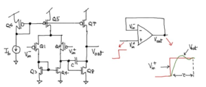
Fig. 1